"Speaking during an event in Phoenix on Friday, Huang lauded TSMC's manufacturing prowess while pandering to US President Donald Trump's America First agenda. "This is the vision of President Trump of reindustrialization - to bring back manufacturing to America, to create jobs, of course, but also this is the single most vital manufacturing industry and the most important technology industry in the world," he said."
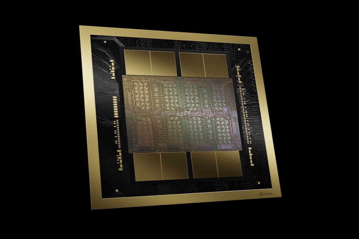
"Modern GPUs are composed of multiple compute and memory dies. The company's Blackwell family of datacenter chips feature two reticle-sized compute dies along with eight stacks of HBM3e memory, all stitched together using TSMC's CoWoS packaging tech. Amkor, an outsourced semiconductor assembly and test services (OSAT) provider, is working on building an advanced packaging plant in the US capable of stitching together silicon dies using TSMC's chip-on-wafer-on-substrate (CoWoS) tech."
TSMC's Arizona Fab21 produced Nvidia's first Blackwell wafer, marking the start of US manufacturing for the company's latest datacenter silicon. Jensen Huang celebrated the wafer and linked the move to President Trump's vision of reindustrialization and job creation. High-end Blackwell GPUs use multiple compute dies and stacks of HBM3e memory that are stitched together with TSMC's CoWoS packaging, which is currently located in Taiwan. Amkor is building a CoWoS-capable advanced packaging plant in the US, with completion expected in 2027 or 2028 and TSMC confirming ground breaking. Some Blackwell SKUs, such as the 96GB RTX Pro 6000, do not use a single-GPU-die design.
Read at Theregister
Unable to calculate read time
Collection
[
|
...
]