"Not long after rejoining Intel in 2021, former CEO Pat Gelsinger announced an ambitious plan to reinvent the chipmaker as a contract semiconductor manufacturing powerhouse. Four years later, Gelsinger has moved on, but his dream is still very much alive. Earlier this summer, Intel quietly began operating the first of two new leading-edge wafer fabs located at its Occotilo manufacturing plant in Chandler, Arizona."
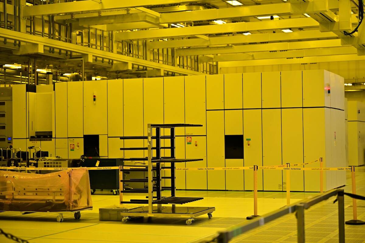
"The facility, which broke ground in late 2021, comprises 600,000 cubic meters of concrete and 110 tons of steel. Access to the heart of the facility is tightly controlled and requires covering oneself head to toe in a cleanroom suit affectionately known as a bunny suit. The awkward getup, which thousands of Intel employees wear everyday, is essential to maintaining the fab's hyper-sterile operating environment, which at any given moment has fewer than 10 particles per cubic foot of air."
Pat Gelsinger rejoined Intel in 2021 and set a plan to transform Intel into a contract semiconductor manufacturer. Intel began operating the first of two new leading-edge wafer fabs at the Ocotillo plant in Chandler, Arizona earlier this summer. Fab52 is producing chips using the 18A process node. The facility broke ground in late 2021 and contains 600,000 cubic meters of concrete and 110 tons of steel. Access is tightly controlled and requires full cleanroom suits. The fab maintains fewer than 10 particles per cubic foot of air. Fab42 uses amber lighting to limit blue light for lithography, and automated carts transport wafers across 30 miles of track.
Read at Theregister
Unable to calculate read time
Collection
[
|
...
]