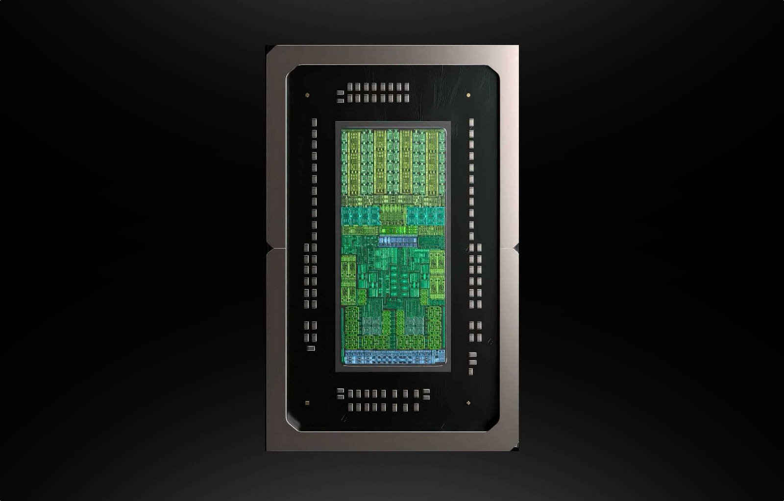
"Fabbed on TSMC's 3nm manufacturing tech, the GB10 is composed of two distinct compute dies: a CPU tile designed by MediaTek, and a GPU tile designed by Nvidia. These two dies are stitched together using TSMC's 2.5D advanced packaging tech and connected via Nvidia's proprietary NVLink Chip-to-Chip interconnect, which provides 600GB/s of bidirectional bandwidth. The CPU die or S-die houses 20 Arm v9.2 cores across two clusters in a big-little arrangement with an equal number of X925 and Cortex A725 cores."
"Details on the GB10's graphics die or G-die, unfortunately, remain rather thin. Nvidia tells us that the chip will deliver roughly 1 petaFLOP of peak FP4 performance with sparsity or about 31 teraFLOPS of single precision compute (FP32). That puts the GB10's, and by extension the Spark's, AI performance roughly on par with an RTX 5070, which we'll note has an MSRP of about $550. However, floating point performance doesn't tell the full story."
GB10 is a miniaturized superchip composed of two compute dies: a MediaTek-designed CPU tile and an Nvidia-designed GPU tile, packaged using TSMC's 2.5D advanced packaging and fabricated on 3nm. The CPU S-die contains 20 Arm v9.2 cores across big-little clusters with X925 and Cortex A725 cores, supported by 32MB of L3 and 16MB of L4 cache. The GPU G-die targets roughly 1 petaFLOP peak FP4 with sparsity and about 31 teraFLOPS of FP32. The CPU and GPU connect via Nvidia's NVLink Chip-to-Chip at 600GB/s bidirectional bandwidth. The GB10 delivers RTX 5070–level AI performance while operating at around 140 watts and includes 128GB of memory.
Read at Theregister
Unable to calculate read time
Collection
[
|
...
]