"Two-dimensional materials exhibit exceptional electronic properties even at monolayer thickness, and the van der Waals heterostructure18,19 enables fine-tuning of the electronic bands20. These characteristics have enabled 2D electronics to extend the scaling ability beyond that of Si technology and create fundamental device mechanisms."
"As one such demonstration of semiconductor devices for integrated circuits, 2D flash memory demonstrates Fowler-Nordheim tunnelling programming speed21,22,23,24 and channel length scaling25 advantages over Si flash memory (mainstream non-volatile memory technology). In recent years, the integration of 2D semiconductors has been increasingly considered by both industry and academic11,12 researchers of integrated circuits. The next stage of 2D electronics should demonstrate its superiority at the system level and accelerate the transition of emerging devices from lab to fab28,29."
"However, 2D semiconductors are currently unable to realize logic circuits comparable to those based on state-of-the-art Si technology. The combination of 2D electronics with mature Si CMOS logic circuits represents a promising way to demonstrate the superiority of 2D electronics at the system level. The pioneering works mainly combine 2D materials with CMOS to improve the function of cell performance, such as using an Si transistor to improve the reliability of 2D memristors14 or using graphene to broaden the spectral range of sensors30. The 2D electronics should further use the CMOS platform to construct superior systems with abilities beyond those of existing technologies."
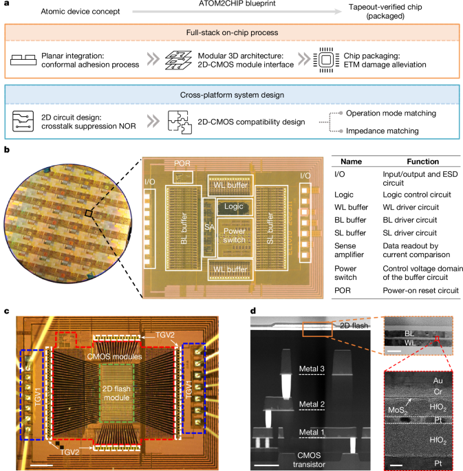
"The essential technology to migrate the advantages of the 2D device concept to the system is lacking, and developing such a systematic procedure and design methodology is extremely difficult. This should include a full-stack on-chip process from planar integration, 3D architecture, to chip packaging and a cross-platform system design to assimilate 2D electronics to the CMOS platform."
Two-dimensional materials exhibit exceptional electronic properties at monolayer thickness and van der Waals heterostructures enable precise band engineering. These properties allow 2D electronics to extend scaling beyond silicon and enable novel device mechanisms. 2D flash memory demonstrates Fowler–Nordheim tunnelling programming speed and channel-length scaling advantages compared with silicon flash memory. Industry and academic groups increasingly consider integrating 2D semiconductors into integrated circuits. System-level demonstrations are required to show superiority and to accelerate transition of emerging devices to fabrication. Combining 2D electronics with mature Si CMOS logic provides a practical route to build superior systems, but full-stack processes and cross-platform methodologies are lacking.
Read at Nature
Unable to calculate read time
Collection
[
|
...
]