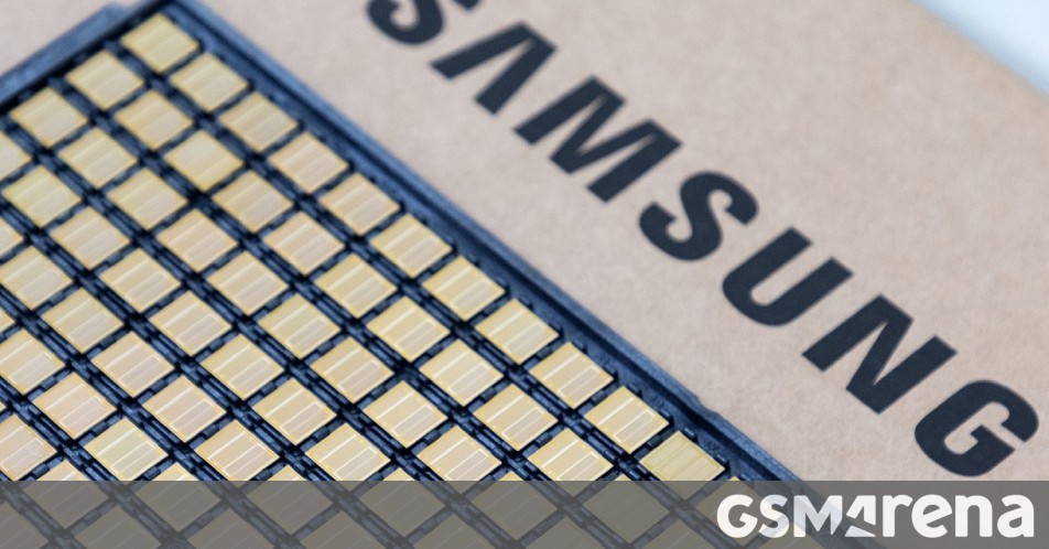
"HBM4 chips are fabbed on a 6th generation of a 10nm-class DRAM process called "1c". Note that DRAM isn't like a CPU core, so the nodes aren't comparable. The HBM4 products also use a 4nm logic base die for higher performance. To put some numbers to it, HBM4 can deliver speeds of 11.7Gbps - per pin! This surpasses the industry standard, which is set at 8Gbps, by 46%."
"Since there are 2,048 pins the total bandwidth is a massive 3.3 terabytes per second. This is a 2.7x increase over HBM3E. Note that when it standardized HBM4, JEDEC (the governing body for computer RAM) decided to reduce per-pin bandwidth compared to HBM3E (9.6Gbps) while doubling the number of pins from 1,024 to 2,048. This was done for improved power efficiency and better thermal management."
Samsung has begun mass production and shipped initial HBM4 memory to customers. HBM4 chips use a 6th-generation 10nm-class DRAM process called "1c" and a 4nm logic base die for higher performance. HBM4 achieves 11.7Gbps per pin, exceeding the JEDEC HBM4 target and the HBM3E per-pin speed, and uses 2,048 pins to reach 3.3 terabytes per second total bandwidth, a 2.7x increase over HBM3E. Samsung currently offers 12-layer stacks in 24–36GB capacities and may introduce 16-layer 48GB designs. Low-voltage TSVs and a power distribution network cut power use by 40% and improve thermal characteristics. Samsung plans to expand production as sales are expected to triple versus 2025, with HBM4E samples slated for second-half 2026 and custom HBM samples to customers next year.
Read at GSMArena.com
Unable to calculate read time
Collection
[
|
...
]