"A tensor processing unit (TPU) is an application-specific integrated circuit (ASIC) that is specifically designed for the purpose of accelerating high-volume mathematical and logical processing tasks that are typically involved with machine learning (ML) workloads. These were designed back in 2015 by Google and released for third-party use in 2018. The first TPUs were designed back in 2015 by Google and released for third-party use in 2018."
"The Ironwood TPU is a seventh-generation chip designed for AI inference workloads, featuring 4,614 teraflops of peak compute, 192 GB of HBM memory, and 7.2 TB/s of memory bandwidth per chip. Scaled up to a pod of 9,216 chips, it delivers 42.5 exaflops of compute power and features a 1.2 TB/s bidirectional interconnect network. It also includes a specialized "SparseCore" to accelerate large-scale data tasks like those in recommendation systems."
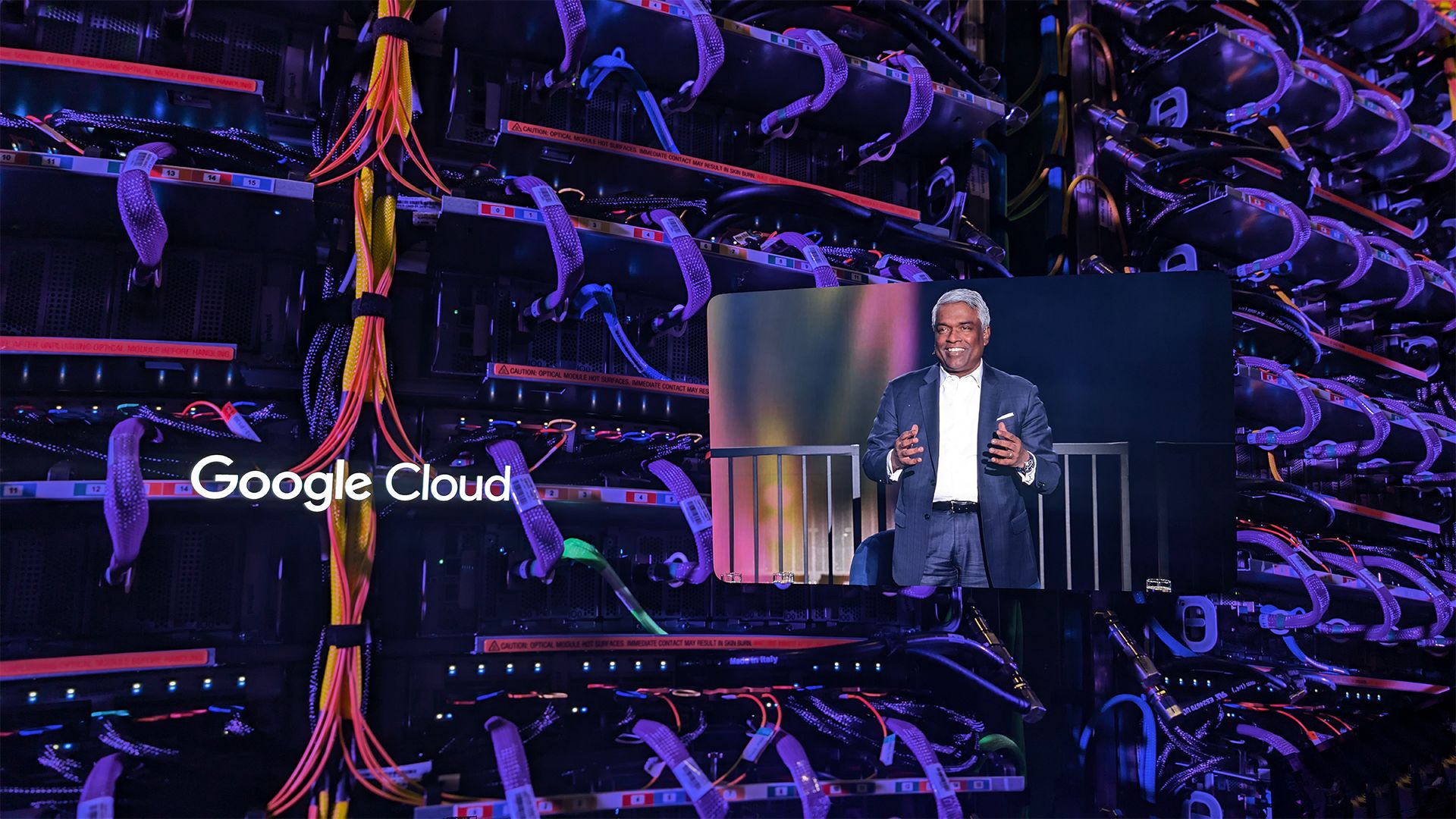
Tensor Processing Units are application-specific integrated circuits designed to accelerate large-scale mathematical and logical operations in machine learning workloads. Google designed the first TPUs in 2015 and released them for third-party use in 2018. Generational improvements expanded TPUs from modest accelerators to supercomputer-scale pods, with early versions focused on inference and later training under limited precision and high throughput. Google improved memory bandwidth, chip count, interconnects, and energy efficiency to serve growing demand for generative AI. The seventh-generation Ironwood TPU targets inference with 4,614 teraflops, 192 GB HBM, 7.2 TB/s per chip, and scales to 42.5 exaflops in a 9,216-chip pod, including a SparseCore for recommendation workloads. Ironwood will be generally available toward the end of 2025.
Read at IT Pro
Unable to calculate read time
Collection
[
|
...
]